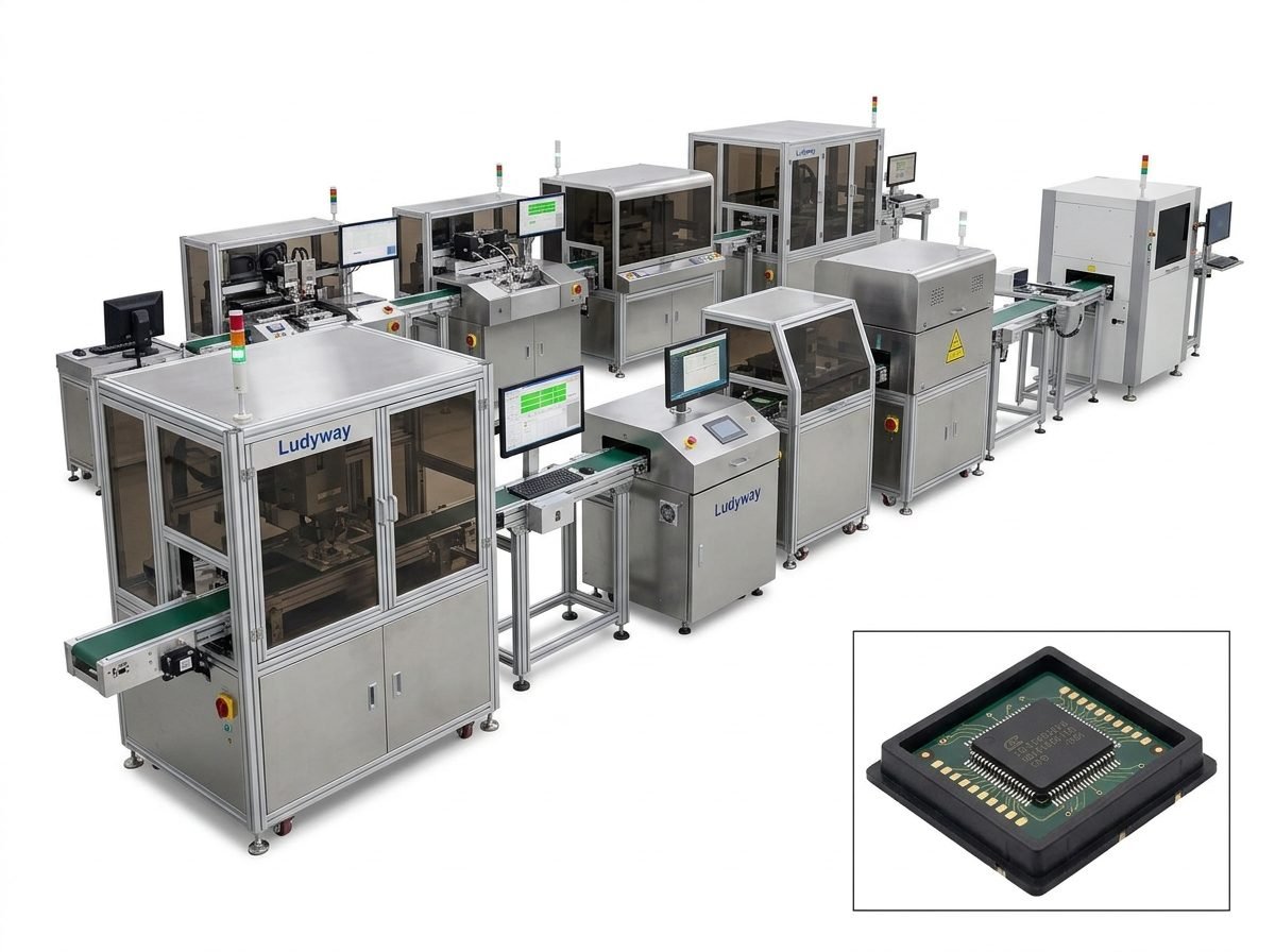
High-Speed Automated Semiconductor Packaging Lines for Advanced IC Assembly
Ludyway Machinery introduces its state-of-the-art High-Speed Automated Semiconductor Packaging Lines, engineered to meet the rigorous demands of modern Integrated Circuit (IC) assembly. These advanced turnkey systems represent a significant leap forward in packaging technology, designed to deliver unparalleled precision, throughput, and reliability for the semiconductor manufacturing sector. Built upon decades of engineering excellence in automation, our packaging lines integrate cutting-edge robotics, vision inspection, and process control to ensure flawless operation and exceptional yield rates. This solution is tailored for manufacturers seeking to scale production, enhance product quality, and reduce total cost of ownership in a highly competitive global market.
Product Features
Our semiconductor packaging lines are distinguished by several key technological advancements that set them apart in performance and efficiency.
Ultra-High Precision Placement and Bonding: The system incorporates advanced servo-driven pick-and-place mechanisms and high-accuracy bond heads, ensuring micron-level placement accuracy for delicate die and substrates. This precision is critical for advanced packaging formats like Fan-Out Wafer-Level Packaging (FOWLP) and 3D IC integration.
Fully Integrated Vision Guidance System: A multi-camera vision system with AI-powered algorithms performs real-time component inspection, alignment correction, and defect detection. This guarantees near-zero defect rates and maximizes production yield by identifying and rejecting faulty components at the earliest stage.
Modular and Scalable Architecture: The production line is designed with a modular framework, allowing for easy integration of additional process modules—such as epoxy dispensing, curing ovens, or laser marking—and straightforward scalability to match evolving production volumes and technological requirements.
Closed-Loop Process Control & Data Analytics: Equipped with sophisticated sensors and IoT connectivity, the system provides real-time monitoring of all critical parameters (force, temperature, pressure). This data is fed into a central Manufacturing Execution System (MES) for predictive maintenance, process optimization, and full traceability.
Designed for Cleanroom Compatibility: All components and materials are selected and designed to meet stringent ISO Class 5-7 cleanroom standards, minimizing particulate contamination and ensuring compatibility with sensitive semiconductor manufacturing environments.
Technical Specifications
| Parameter |
Specification |
| Maximum Throughput |
Up to 60,000 Units Per Hour (UPH) |
| Placement Accuracy |
±10 µm @ 3 Sigma |
| Supported Substrate Sizes |
2″ x 2″ to 12″ x 12″ (Customizable) |
| Bonding Force Range |
0.1 kg – 15 kg (Programmable) |
| Vision System |
High-Resolution CCD with AI Defect Classification |
| Control System |
Industrial PC with Proprietary HMI & MES Interface |
| Power Requirements |
380-480V AC, 3-Phase, 50/60 Hz |
| Compressed Air |
0.6 – 0.8 MPa, Clean & Dry |
| Footprint (Standard Line) |
Approx. 8m (L) x 3.5m (W) |
| Cleanroom Class |
Compatible with ISO Class 5-7 |
Application Fields
Ludyway’s High-Speed Automated Semiconductor Packaging Lines are versatile solutions engineered for a broad spectrum of advanced assembly applications within the electronics industry.
Advanced IC Packaging: Ideal for high-volume production of complex packages including System-in-Package (SiP), Flip-Chip, 2.5D/3D ICs, and Fan-Out Wafer-Level Packaging (FOWLP).
Power Device Assembly: Provides reliable die attach and encapsulation for power semiconductors, IGBT modules, and wide-bandgap (SiC/GaN) devices used in automotive, renewable energy, and industrial drives.
Sensor and MEMS Packaging: Handles the delicate assembly requirements of MEMS sensors, optical devices, and RF components with high precision and cleanliness.
LED and Optoelectronics: Automates the die bonding and packaging processes for high-brightness LED chips and optoelectronic components, ensuring consistent light output and performance.
Consumer Electronics and Automotive Electronics: Supports the mass production of chipsets, processors, and control units for smartphones, tablets, automotive ADAS systems, and infotainment, where reliability and miniaturization are paramount.